When a semiconductor packaging engineer specifies a D50 of 5 microns and a D98 below 15 microns for their EMC silica filler, they are not being conservative. Those numbers are the exact threshold between a molding compound that flows reliably into fine-pitch cavities and one that causes short shots, wire sweep, and field failures. The same applies to PCB laminates: a single oversized silica particle can create a void at the resin-filler interface that disrupts signal integrity in a 5G application running at 28 GHz.
Tight particle size control in fused silica filler is not a quality assurance detail — it is a functional requirement. This article explains the three specific failure modes that poor PSD control causes, how to read and specify a silica filler PSD correctly, and what the processing steps look like that make the difference between broad and tight distributions.
At EPIC Powder Machinery, we supply electronics-grade fused silica and quartz powder for EMC and PCB applications, with real-time laser diffraction monitoring on every production run and a full Certificate of Analysis with every shipment.
What ‘Tight Particle Size Control’ Actually Means in Practice
A silica filler PSD is defined by at least three numbers: D50 (median size), D90 or D98 (the coarse end of the distribution), and sometimes D10 (the fine end). Each number controls a different aspect of your formulation’s behaviour.
| PSD Parameter | What It Measures | What It Controls in EMC/PCB | Typical Target Range |
| D10 | 10% of particles are finer than this size | Minimum filler size — excess fines increase surface area and raise viscosity | 0.5 – 2 microns (application-dependent) |
| D50 | Median particle size | Packing density and baseline viscosity | 3 – 10 microns for standard EMC; 1 – 5 microns for advanced packages |
| D90 | 90% of particles are finer than this | Intermediate coarse fraction control | 15 – 30 microns depending on mold geometry |
| D98 / D99 | 98-99% of particles are finer than this | Near-maximum particle size — killer particle control | Below 20 microns standard; below 10 microns for advanced packages |
| Dmax / D100 | Absolute maximum particle size present | Hard limit — no particle above this value | Below 45 microns standard; below 25 microns fine-pitch; below 15 microns ultra-fine |
| Span = (D90-D10)/D50 | Width of the distribution | Distribution uniformity — lower span = tighter distribution | Below 2.0 for standard EMC; below 1.2 for high-density packaging |
The most commonly misspecified parameter is Dmax — the absolute maximum particle size. D90 and D98 are statistical measures; they tell you about 90% or 98% of the particles, but they say nothing about the remaining 2% that are larger. For EMC and PCB applications, that 2% is where failures originate. A silica filler with D98 = 18 microns could still contain particles at 50-80 microns if Dmax is not separately specified and controlled. Specifying D98 and Dmax as separate numbers closes this gap.
Three Failure Modes That Poor PSD Control Causes
1. Viscosity Spikes and Short Shots (the Fines Problem)
When a silica filler has too many ultra-fine particles — D10 below 0.3 microns, or a long fine tail in the distribution — the total surface area of the filler increases sharply. Resin wets filler surfaces, so higher surface area means more resin is consumed keeping particles suspended and lubricated. The result is a viscosity increase that can be severe: a shift from D10 of 1 micron to D10 of 0.3 microns at the same loading can increase EMC compound viscosity by 40-60%.
At standard transfer moulding temperatures, this higher viscosity means the compound cannot fully penetrate fine-pitch mould cavities before it begins to gel. The result is incomplete fill — short shots — with voids in the finished package. Short-shot rates of 5-15% are common in EMC lines that have not controlled the fine tail of their silica PSD.
The fix is controlling D10 and setting an upper limit on the fines fraction (the percentage of material below 1 micron). This requires either a multi-stage classification process that strips ultra-fines from the product, or a grinding process that avoids generating them in the first place.
2. Wire Sweep and Delamination (the Coarse Particle Problem)
On the coarse end, oversized particles cause two distinct failure modes. The first is wire sweep: during transfer moulding, the flowing EMC compound exerts hydraulic force on the fine wire bonds connecting the die to the package substrate. A large, rigid silica particle (say, 80 microns in a compound specified for D90 = 30 microns) can physically deflect a 20-micron gold wire bond as the compound flows past. Wire sweep above 5-10% of wire diameter is a reliability failure.
The second failure mode is delamination. Large particles concentrate stress in the cured composite — when the package undergoes thermal cycling (from -55 to +125 degrees C in automotive qualification, for example), the stress concentrations around large particles exceed the adhesion strength of the resin-filler interface. Cracks initiate at these particles and propagate, eventually causing delamination between the EMC and the die attach or substrate.
Both failures are prevented by hard Dmax control — not just D90 or D98. A vibratory sieve at the correct aperture plus a downstream air classification step that removes any material above the target Dmax provides the necessary hard upper limit.
3. CTE Mismatch and PCB Warpage (the Uniformity Problem)
Silicon has a Coefficient of Thermal Expansion (CTE) of approximately 3 ppm per degree C. FR-4 glass-epoxy PCB substrate has a CTE of around 14-17 ppm per degree C. The purpose of the silica filler in the PCB laminate is to bridge this gap — the filler reduces the CTE of the composite toward the silicon value, reducing the stress on solder joints during thermal cycling.
This CTE reduction is proportional to filler loading. Higher loading = lower composite CTE = better CTE match to silicon = longer solder joint life. But high loading only works if the PSD allows it. A broad, poorly controlled PSD produces inefficient particle packing — larger particles create voids that cannot be filled by smaller ones because the size ratio is wrong. Maximum achievable loading drops from 85-90% (tight bimodal PSD) to 65-75% (broad uncontrolled PSD), with a corresponding loss of CTE reduction.
The result is a PCB laminate with higher-than-designed CTE, which shows up as warpage during reflow soldering (the ‘popcorn effect’ in packages, board bowing in bare PCBs) and premature solder joint fatigue in field service.
| Quick Specification Reference: Silica Filler PSD by ApplicationStandard EMC (QFP, SOP packages): D50: 5-10 microns | D98: <25 microns | Dmax: <45 microns | Loading: 70-80% Fine-pitch EMC (BGA, flip-chip): D50: 3-6 microns | D98: <15 microns | Dmax: <25 microns | Loading: 75-85% Ultra-fine EMC (advanced wafer-level packaging): D50: 1-3 microns | D98: <8 microns | Dmax: <12 microns | Loading: up to 90% PCB laminate filler (standard FR-4 replacement): D50: 5-15 microns | D90: <35 microns | Dmax: <50 microns | Loading: 60-75% Glob top encapsulant: D50: 3-8 microns | D98: <20 microns | Narrow span (<1.5) critical for viscosity stability Note: Specifications vary by package design, wire bond pitch, and resin system. Confirm with your formulation team. |
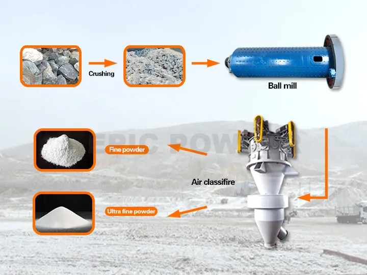
How Tight PSD Is Achieved in Fused Silica Production
Achieving and maintaining the PSD specifications above requires control at four stages of the production process. Each stage adds a layer of assurance; none of them alone is sufficient.
1. Raw Material Control
Fused silica feedstock quality determines what is achievable in subsequent processing. Inconsistent raw material density, moisture content, or impurity level forces the processing equipment to operate outside its optimal parameters, which broadens the output PSD. All incoming fused silica feedstock should be tested for SiO2 purity (target above 99.7% for electronics grade), bulk density, and pre-milling PSD before entering the production process.
2. Precision Milling — Closed-Circuit Grinding
For electronics-grade silica, closed-circuit grinding is the standard. The mill and classifier operate in a continuous loop: the mill reduces particle size, the classifier immediately sorts particles into fine (on-spec, exits the circuit) and coarse (rejected, returned to the mill). This prevents overgrinding of already-fine particles and ensures that only material meeting the size specification accumulates in the product stream.
Jet milling is commonly used for the finest grades (D50 below 5 microns) because it provides high energy input for size reduction without metal contamination — the compressed air grinding principle means no mill surfaces contact the product. For coarser grades (D50 5-15 microns), ball mill or ring roller mill in closed circuit with an air classifier is more energy-efficient.
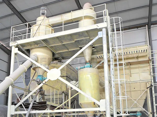
3. Multi-Stage Air Classification
A single classification stage separates fine from coarse but produces a gradual transition zone rather than a sharp step function. For electronics-grade silica where Dmax must be hard-limited, multi-stage classification is needed: a primary classifier sets the D50, and a secondary classifier specifically targets the coarse tail — removing material above the Dmax threshold with high efficiency.
Horizontal air classifiers provide sharper separation than vertical designs because the particle trajectory in a horizontal flow field is less affected by gravitational settling of larger particles. For D98 specifications below 15 microns — the range required for advanced EMC — horizontal classifier geometry is the standard choice.
4. Real-Time Laser Diffraction Monitoring
The output PSD must be verified continuously during production, not just at the start of a batch. In-line laser diffraction sensors measure the product stream every 30-60 seconds. If D50 drifts by more than 5% from the target, or if D98 shows an upward trend, the system alerts the operator for an immediate classifier parameter adjustment.
This continuous monitoring is the only way to guarantee that the first bag of a production run and the last bag have identical PSDs. Batch-end sampling — checking one sample after 4-8 hours of production — misses intra-batch variation that can be significant in long production runs.
Frequently Asked Questions
What is the difference between angular and spherical silica for EMC and PCB fillers?
The difference is fundamental to how the filler behaves in the resin system. Spherical silica particles act like ball bearings in the compound — they rotate freely past each other, allowing high filler loading (up to 85-90% by weight) without the viscosity becoming unworkable. This high loading is what achieves the CTE reduction required to match silicon.
Spherical silica is produced by flame spheroidisation or sol-gel synthesis and is more expensive than angular silica. Angular silica is produced by crushing and grinding, which creates irregular, jagged shapes. The interlocking of angular particles in the cured composite improves mechanical adhesion between filler and resin, which increases flexural strength and crack resistance. The trade-off is significantly higher viscosity at the same loading, which limits how much filler you can incorporate. For most modern EMC applications where CTE control is the priority, spherical silica is the default choice. Angular silica is used where mechanical strength or lower cost is the primary driver.
How does silica filler PSD affect dielectric constant (Dk) in PCB laminates?
The dielectric constant of a PCB laminate is a volume-weighted average of the Dk values of its components. The epoxy resin (Dk approximately 4.0), the silica filler (Dk approximately 3.8 for fused silica), and any voids or air pockets (Dk = 1.0). Air pockets are the key variable. When silica filler PSD is broad or poorly controlled, particle packing is inefficient and voids form at the resin-filler interface. These voids lower the composite Dk below the designed value and, critically, cause lot-to-lot Dk variation. It’s because that the void fraction changes with each batch. Tight PSD control — specifically, controlling the span value so that particle packing density is consistent. This minimises void formation and stabilises Dk from lot to lot. For 5G mmWave applications at 28 GHz and above, Dk variation of more than +/- 0.05 is enough to detune antenna elements and fail the electrical specification.
Bột Epic
Bột Epic, 20+ years of experience in the ultrafine powder industry. Actively promote the future development of ultra-fine powder, focusing on crushing, grinding, classifying and modification process of ultra-fine powder. Contact us for a free consultation and customized solutions! Our expert team is dedicated to providing high-quality products and services to maximize the value of your powder processing. Epic Powder—Your Trusted Powder Processing Expert!

Cảm ơn bạn đã đọc. Tôi hy vọng bài viết của tôi có ích. Vui lòng để lại bình luận bên dưới. Bạn cũng có thể liên hệ với đại diện khách hàng trực tuyến của EPIC Powder Zelda để biết thêm bất kỳ thông tin nào khác.”
— Jason Wang, Engineer